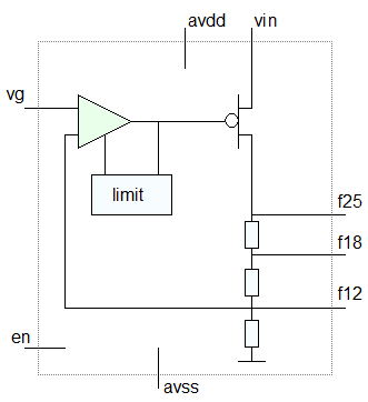
Features
- Input voltage range 2.9V – 4.3V.
- Output voltage 1.2V – 2.5V.
- Output voltage and current can be customized.
- Output short circuit and fold-back protection.
- Switchable over-temperature protection.
- Universal design works with a wide variety of pad libraries.
- Works with OT0102bh voltage and current band gap.
- External 4.7µF decoupling capacitor.
- Power down/enable input.
- Fast response to current steps.
- Good line and load regulation.
- -40°C to 120°C temperature operation.
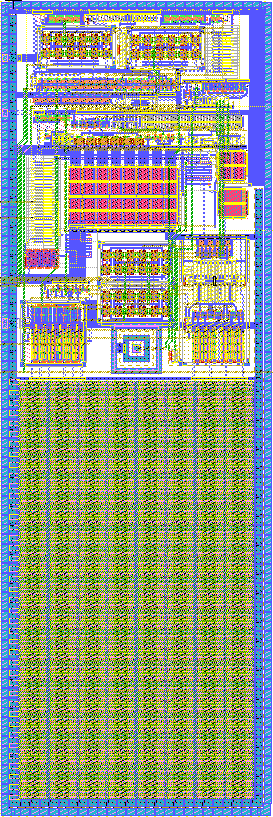
- Base cell area < 0.1mm2 in 0.35µ CMOS.

Typical Applications
- Battery to 1.2V, 1.8V, or 2.5V core VDD rails.
- 3.3V to 1.2V, 1.8V, or 2.5V VDD rails.
Deliverables
- Flat GDS.
- LEF.
- LVS netlist.
- Integration notes.
- Production test notes.
Service
- 4 Weeks lead time for process ports.
- Available support for manufacturing and characterization.
- Available translation to your design style.
- Available on-site design review.
- Source licensing available.
